M.E in Electronics and Communication (VLSI Design) is a two-year postgraduate programme that aims to convey knowledge of VLSI system design, covering algorithms, Architectures, Physical designs, Verification Systems, simulation and low power design techniques etc. The new developments in VLSI design have aided most systems to develop compacted and reliable. With the advent of VLSI designs, the number of applications of integrated circuits (ICs) in high-performance computing, telecommunications, image and video processing, and consumer electronics has been growing at a fast. With advances in technologies like feature and product innovations, there is a constant need to design and develop integrated circuits. Since products like mobile phones are being released with new features in increasingly shorter cycles, there is a healthy demand for qualified very large-scale integration (VLSI) engineers to work on these products. Therefore, there is good scope and high demand for engineers in the fast-changing chip designing industry.
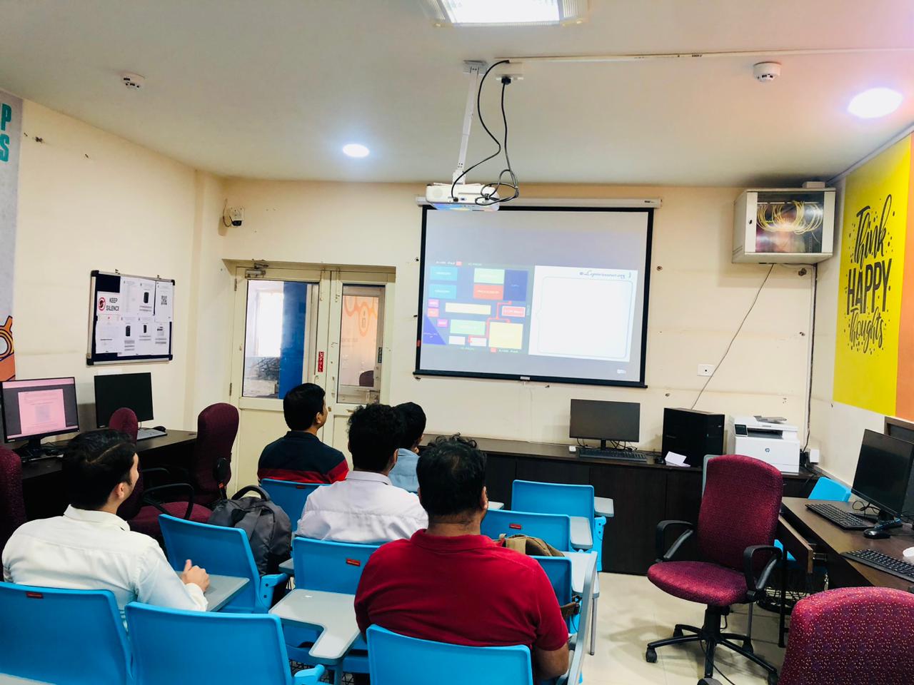
The program emphasizes hands-on experience with industry-standard tools and labs, preparing students for real-world challenges in designing complex ICs. The program provides an interdisciplinary approach, combining hardware and software knowledge for solving complex problems in the industry. Students will gain hands-on experience with leading VLSI design tools like Xilinx, AMD, Cadence, Synopsys, and Mentor Graphics to prepare for professional practice.
Students will also engage in internships, industrial visits, and partnerships with global semiconductor companies, providing real-world exposure.
Students will have good opportunities in global placement demands in semiconductor industries and core electronics chip manufacturing.
Program Outcomes
- An ability to independently carry out research /investigation and development work to solve practical problems.
- An ability to write the present substantial technical report/documents.
- Students should be able to demonstrate a degree of mastery over the area as per the specialization of the program. The mastery should be at a level higher than the requirements in the appropriate bachelor program.
Program Specific Outcomes
- Students will acquire the ability to design, implement and analyse integrated circuits and systems using modern VLSI design methods.
- Students will be competent enough in Electronic Design Automation (EDA) tools for front-end and back-end VLSI design digital/analogy integrated circuits with optimal performance.
- Students will be capable of integrating VLSI design in real time research problems/ applications and contribute to solve real time problems in the field of VLSI and semiconductor.
Program Educational Objectives
- Impart knowledge/skill in the areas of Semiconductor Chip Design, Synthesis, Verification, Manufacturing, and Testing.
- Work in reputed semiconductor based multinational companies, government and research organizations or as an entrepreneur to build novel IC solutions of real-time issues for the nation.
- Able to cope with semiconductor chip design and manufacturing challenges through continuing education, increased responsibility, teamwork and ethical code of conduct.
Cyber Security and Digital Forensics Laboratory

Tokyo
Tokyo is the capital of Japan.


